Multilayer PCB Manufacturing Services
Dense digital, power, and mixed-signal designs depend on multilayer stackups done right. MOZPCB builds 4–32 layer boards with stackup tables, impedance targets, and fabrication notes you can audit—not assume.
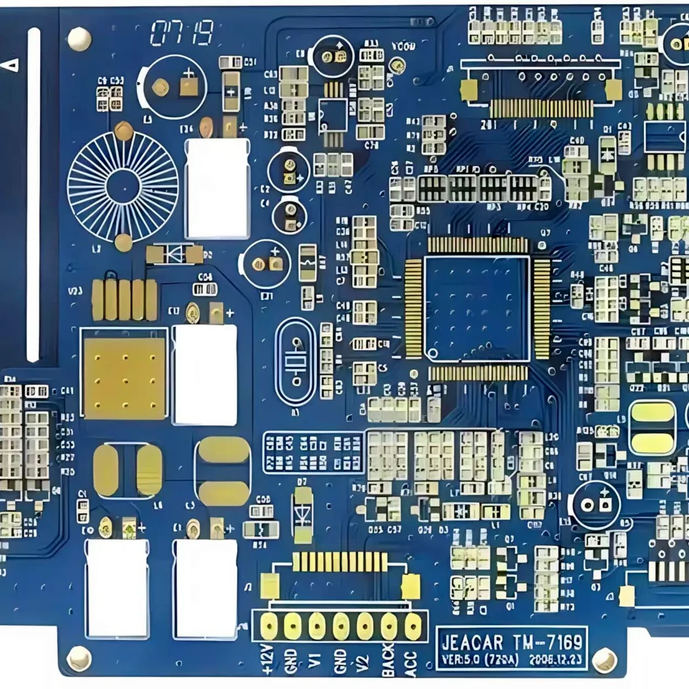
Service overview
Multilayer PCBs stack alternating copper and dielectric into a single laminated construction. Layer count, plane assignment, copper weight, and via architecture determine whether your design routes cleanly and survives reflow, test, and field life. MOZPCB treats multilayer RFQs as stackup problems first: we confirm layer map, impedance references, and copper balance before quoting tooling.
Our multilayer scope spans standard 4–8 layer FR-4 for general electronics through 10–32 layer builds for dense networking, industrial control, and advanced mixed-signal products. When density demands it, multilayer programs can incorporate HDI microvias or hybrid material sets—always reviewed against process capability rather than assumed from a catalog checkbox.
Prototype and small-batch multilayer work is a core use case. Early spins need honest DFM on annular rings, aspect ratio, and plane continuity; production releases need locked travelers and coupon evidence. The same engineering interface carries both.
What we offer
- 4–32 layer rigid multilayer fabrication (construction-dependent)
- Stackup engineering with documented dielectric targets and copper weights
- Controlled impedance builds with tolerance targets and test coupons
- Blind, buried, and through-hole via structures reviewed per design
- HDI microvia options when layer count alone cannot solve escape routing
- Surface finishes matched to assembly pitch and storage requirements
- Copper balance review to reduce bow, twist, and lamination warp risk
- Electrical test: flying probe or fixture-based per job agreement
Technical capabilities
- Standard and high-Tg FR-4 dielectrics; low-loss laminates when specified
- Copper weights from 1 oz through 3 oz and heavier where etch allows
- Impedance control typically ±10%; tighter tolerances reviewed case by case
- Sequential lamination for HDI multilayer when required
- Panelization suited to assembly carriers and depanelization plans
- IPC class alignment documented during RFQ intake
Common applications
- Industrial controllers, PLCs, and motor drives
- Telecom, networking, and enterprise compute mainboards
- Medical and diagnostic electronics with disciplined documentation
- Power conversion and battery management with split plane strategy
- IoT gateways and edge devices with dense mixed-signal routing
How the process works
- 01
Requirements intake
Share Gerber, BOM, drawings, quantities, and any reliability or compliance notes.
- 02
Technical alignment
We confirm materials, finishes, assembly flow, and test expectations with you.
- 03
Production & inspection
Manufacturing and assembly follow the agreed traveler with documented checks.
- 04
Delivery
Packing, labeling, and shipment according to your logistics instructions.
Multilayer fabrication
-
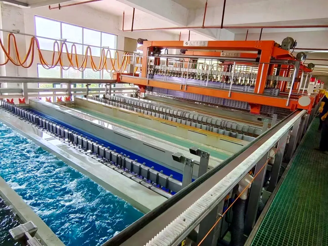
Plating line -
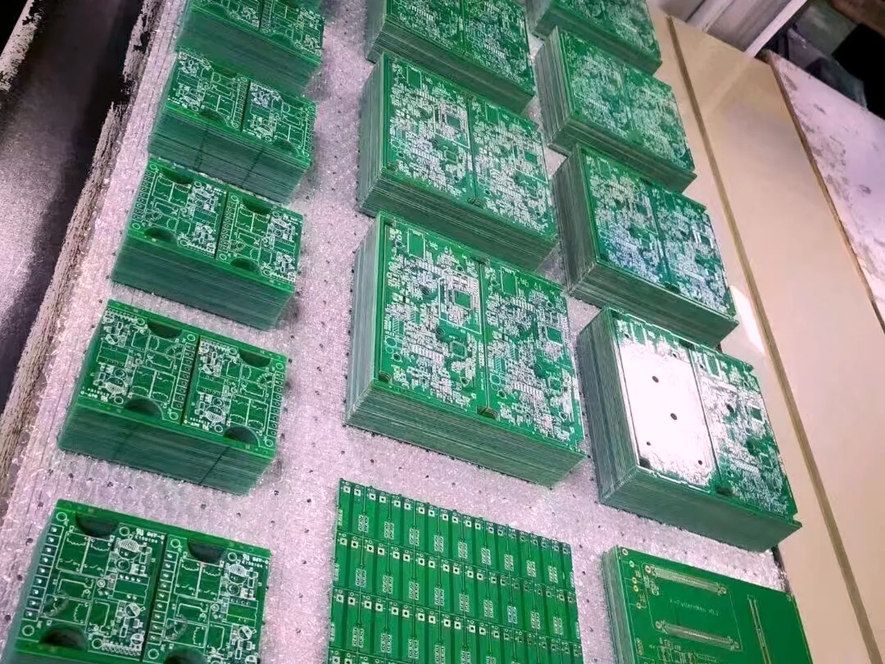
Panelized boards -
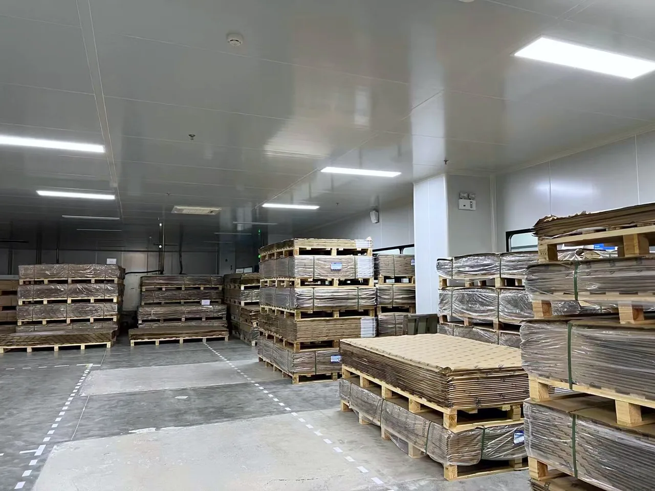
Laminate store
Related services
FAQ
How do I choose the right layer count?
What stackup information should a multilayer RFQ include?
Can you build controlled impedance on multilayer boards?
Do you support multilayer prototypes and production on the same stackup?
Get started
Ready for the next step?
Send your project files and requirements. We will review stackup, assembly, and test needs, then respond with a clear quotation path.