HDI PCB Manufacturing Services
High-density interconnect PCBs help teams shrink package size while maintaining signal integrity. MOZPCB supports advanced stackups where design rules and materials align.
Service overview
HDI designs lean on microvias, tight registration, and disciplined stackup planning. We review your via structures, pad stacks, and sequential lamination assumptions before committing to tooling.
HDI is one of our core specializations rather than an edge case. Every HDI quote includes an engineering review of the via architecture—whether a 1+N+1 build with laser microvias meets your escape routing, or whether stacked and staggered vias in a 2+N+2 or 3+N+3 construction are genuinely required—because each additional lamination cycle adds cost and yield risk.
Applications range from compact wearables to dense networking blades—each with different reliability and thermal constraints we document up front.
What we offer
- HDI structures from 1+N+1 through 3+N+3 and any-layer builds, subject to design review
- Laser-drilled microvias, blind and buried vias, and via-in-pad with fill and cap plating
- Fine line and space processing where mechanical and imaging limits allow
- Stackup engineering for 0.4 mm and 0.5 mm pitch BGA escape routing
- Material sets suited to high-speed or low-loss requirements when specified
- Controlled impedance with documented tolerance targets and test coupons
- Inspection strategies that reflect the defect modes HDI processes see most often
- DFM feedback on pad stacks, aspect ratios, and copper balancing before tooling
Technical capabilities
- Microvia diameters typically 0.1 mm (4 mil) and up, laser-drilled, per stackup review
- Line width and spacing down to 0.075 mm (3 mil) where imaging and copper weight allow
- Multiple sequential lamination cycles (1+N+1, 2+N+2, 3+N+3) subject to design review
- Via-in-pad with resin fill and copper cap plating for dense BGA fields
- Controlled depth routing and via fill requirements documented per job
- Copper balancing recommendations to reduce bow and twist risk
- Low-loss and high-speed laminate options for signal-integrity-driven designs
Common applications
- Consumer electronics with aggressive Z-height limits
- Smartphones, wearables, and hearables with fine-pitch BGA and SiP packages
- Medical and diagnostic instruments requiring dense interconnect
- Communication modules, 5G radios, and antenna-in-package adjacent routing
- Avionics and aerospace instrumentation where weight and density both matter
How the process works
- 01
Requirements intake
Share Gerber, BOM, drawings, quantities, and any reliability or compliance notes.
- 02
Technical alignment
We confirm materials, finishes, assembly flow, and test expectations with you.
- 03
Production & inspection
Manufacturing and assembly follow the agreed traveler with documented checks.
- 04
Delivery
Packing, labeling, and shipment according to your logistics instructions.
In our factory
-
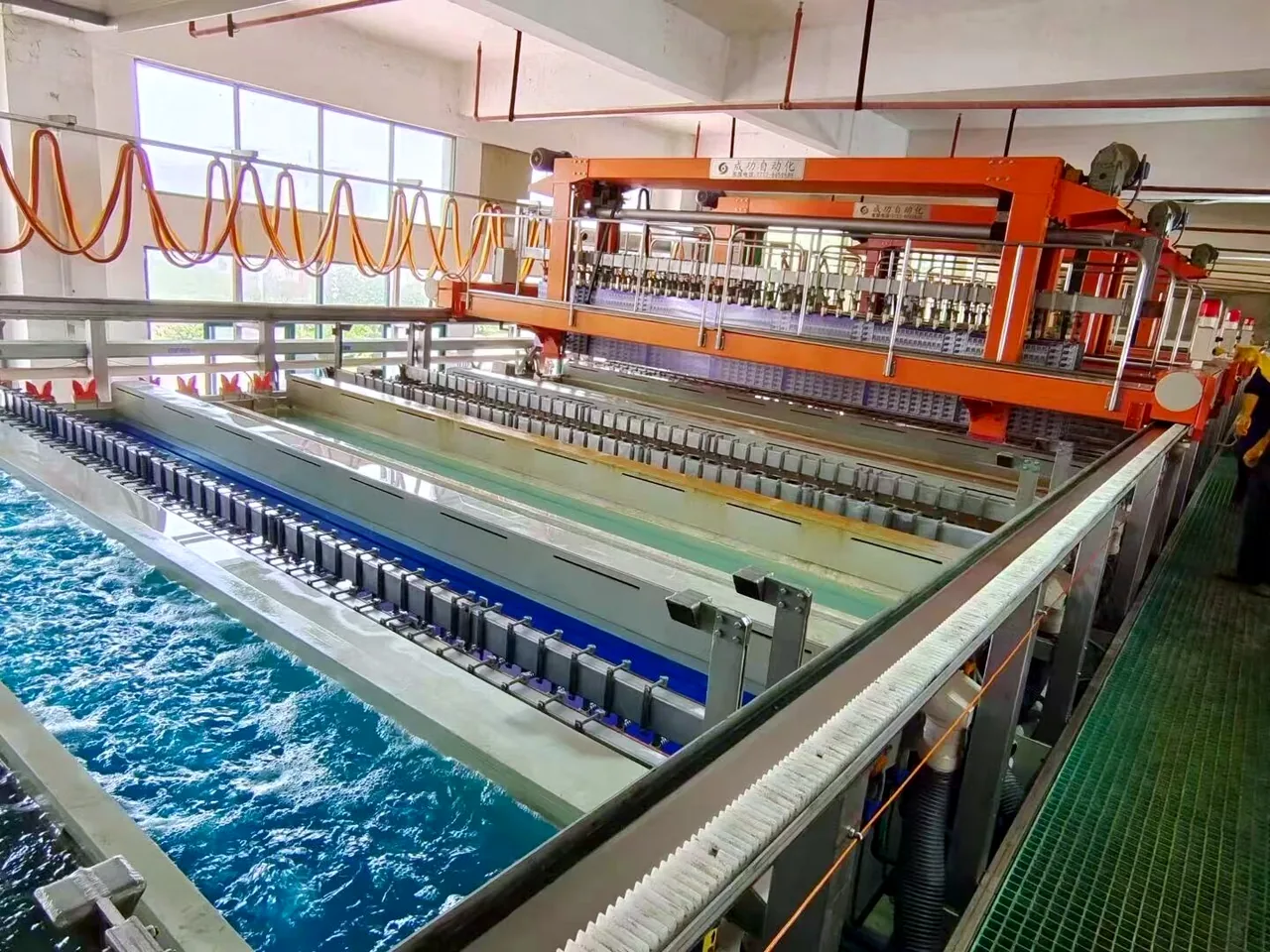
Plating line -
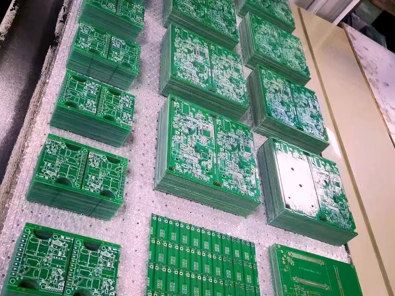
Panelized boards -
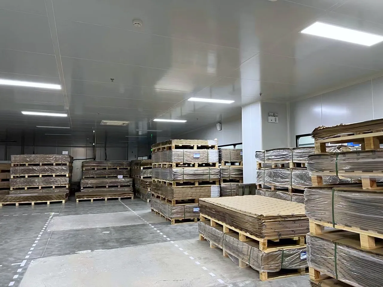
Laminate store
Related services
FAQ
When should I choose HDI instead of a standard multilayer board?
What is the difference between 1+N+1, 2+N+2, and 3+N+3 HDI stackups?
Do you support via-in-pad for BGA designs?
How much does sequential lamination affect HDI PCB cost?
Do you review sequential lamination before quoting?
Get started
Ready for the next step?
Send your project files and requirements. We will review stackup, assembly, and test needs, then respond with a clear quotation path.