Custom PCB Fabrication Services
From quick-turn prototypes to controlled production builds, MOZPCB fabricates rigid, multilayer, HDI, and specialty boards with transparent engineering support—so your quote reflects what will actually be built.
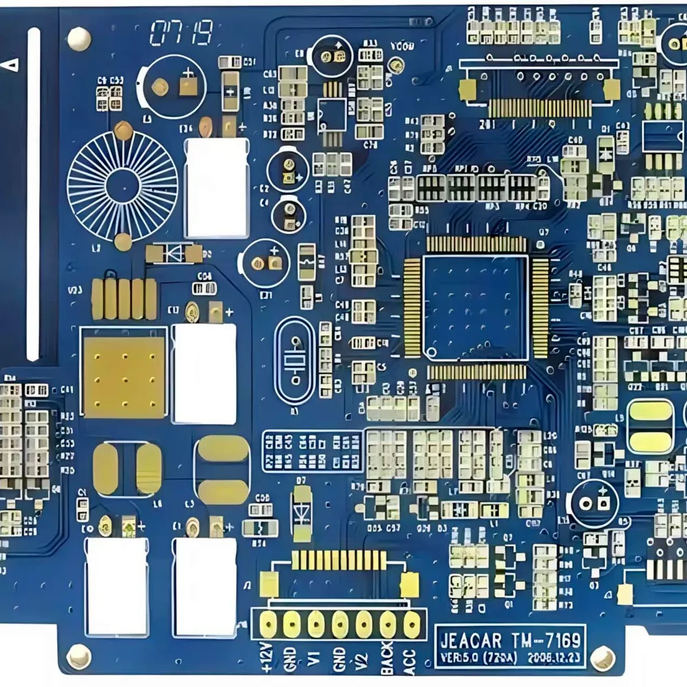
Service overview
PCB fabrication is where design intent meets process capability. Layer count, copper weight, dielectric choice, surface finish, and mechanical outline all interact; a drawing that looks complete can still leave critical decisions open. MOZPCB treats every fabrication RFQ as an engineering intake—not a price-only transaction—so stackup, impedance, and manufacturability are aligned before panels enter production.
Our fabrication scope covers the board types hardware teams use most often: rigid FR-4 for general electronics, advanced multilayer for dense digital and mixed-signal designs, HDI with microvias when escape routing demands it, metal core for LED and power thermal paths, and RF-oriented laminates when controlled dielectric performance is part of the product requirement. Specialty constructions are reviewed case by case against material availability and process windows.
What separates a reliable fab partner from a catalog price sheet is how early problems surface. We flag annular-ring risk, copper imbalance, mask-defined pad conflicts, drill-to-copper clearance issues, and impedance coupon needs during review—so you get a firm path to tooling instead of surprises after the first article. Whether you are spinning an EVT board or releasing a locked pilot lot, the same documentation backbone carries forward.
If your program also needs assembly or turnkey sourcing, fabrication stays coordinated with the PCBA traveler: finish selection, panelization, and test coupon strategy are chosen with downstream reflow and inspection in mind, not in isolation.
What we offer
- Rigid and multilayer PCBs for consumer, industrial, and communications products
- Prototype and small-batch runs with documented process controls and revision traceability
- HDI and fine-feature builds where density, registration, and microvia architecture drive the design
- Metal core and thermally conscious layouts for power conversion and LED modules
- High-frequency and hybrid material options when your stackup targets controlled dielectric performance
- Surface finishes including HASL, lead-free HASL, ENIG, OSP, and immersion silver
- Controlled impedance builds with stackup tables, tolerance targets, and coupon planning
- DFM feedback on spacing, annular rings, mask-defined pads, copper balance, and testability
- Mechanical options: V-score, tab routing, countersinks, and array formats for assembly partners
- Incoming and in-process inspection aligned to your acceptance criteria and IPC class expectations
Technical capabilities
- Board types: rigid, flex, rigid-flex, HDI, metal core (project-dependent)
- Layer counts from 1–2 layer quick turns through multilayer builds up to 32 layers for supported constructions
- Copper weights including 1 oz, 2 oz, 3 oz, and heavier where etch and plating allow
- Dielectrics from standard and high-Tg FR-4 to Rogers/PTFE hybrids when the RFQ specifies them
- Minimum line/space and via structures confirmed per copper weight and imaging capability
- Stackup assistance for controlled impedance, differential pairs, and hybrid material builds
- Solder mask and silkscreen in common colors; legend clarity reviewed against fine-pitch fields
- Electrical test: flying probe or fixture-based continuity/isolation per job agreement
- Mechanical routing, scoring, and panelization suited to SMT carriers and depanelization plans
Common applications
- Industrial control, automation, and ruggedized embedded hardware
- IoT gateways, sensors, edge devices, and connected product mainboards
- Power conversion, motor drives, battery management, and LED lighting modules
- Telecom infrastructure, enterprise networking, and RF-adjacent digital boards
- Medical and diagnostic electronics requiring disciplined documentation and lot control
- Automotive-adjacent and mobility electronics where thermal and vibration margins matter
How the process works
- 01
File and stackup intake
Share Gerber/drill data, layer map, impedance tables, mechanical drawings, and any IPC class or finish constraints. Incomplete packages are clarified before quoting—not after.
- 02
Engineering and DFM review
We check annular rings, clearances, copper balance, finish suitability, and coupon needs, then align on open questions that would otherwise delay tooling.
- 03
Fabrication and in-process checks
Boards are built to the agreed traveler with imaging, plating, lamination, and drill/rout controls appropriate to the construction.
- 04
Test, packing, and handoff
Electrical test and visual inspection per agreement, then protective packing and labeling ready for assembly, inventory, or shipment.
Inside PCB fabrication
-
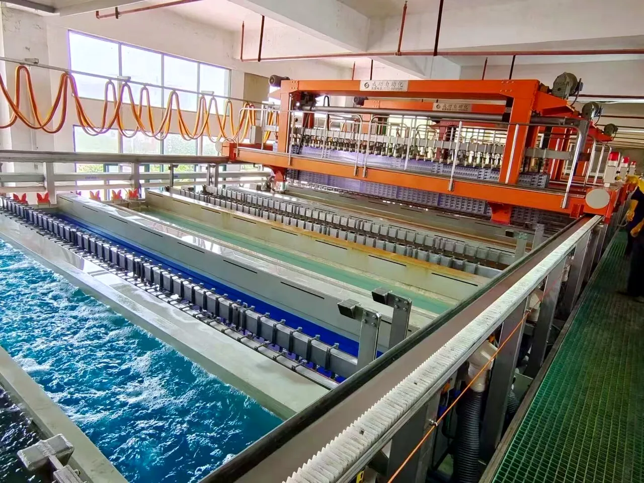
Plating line -
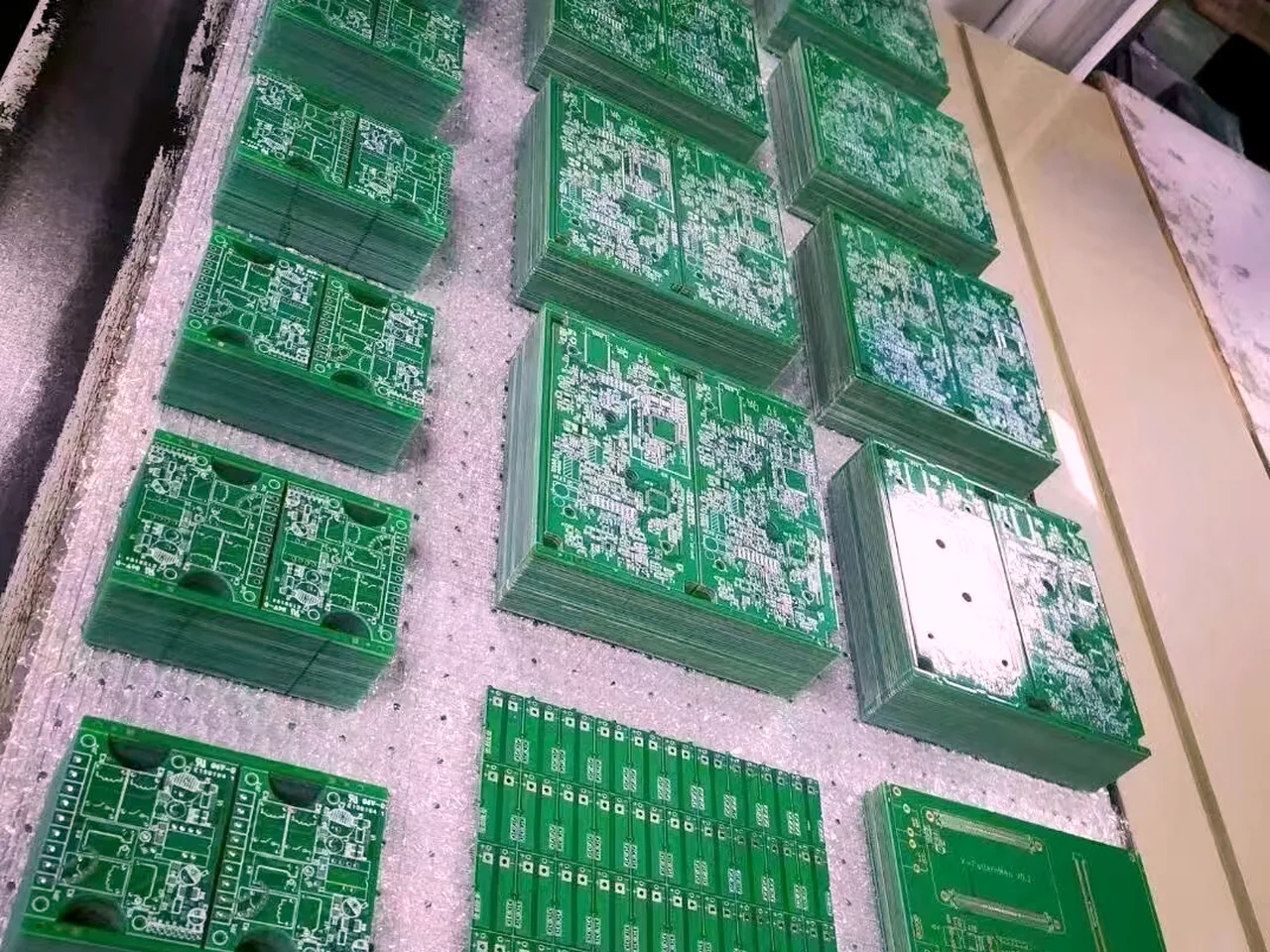
Panelized boards -
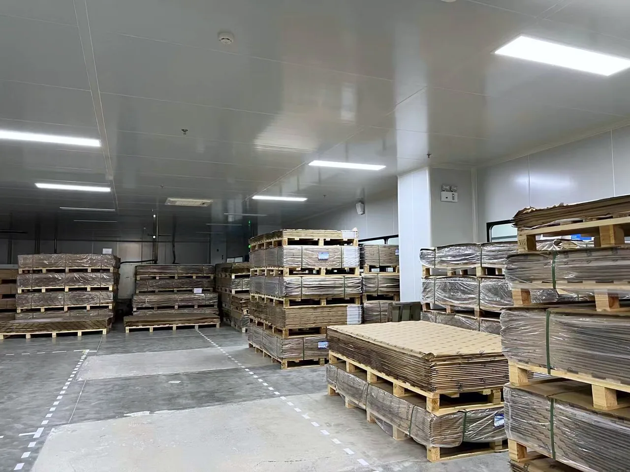
Laminate store
Related services
FAQ
What files do you need for a fabrication quote?
Do you support prototype quantities as well as small-batch production?
Which surface finish should I choose for my PCB?
Can you build controlled-impedance multilayer boards?
How do you handle HDI, metal core, or high-frequency materials?
What inspection and electrical test options are available?
Get started
Ready for the next step?
Send your project files and requirements. We will review stackup, assembly, and test needs, then respond with a clear quotation path.