Controlled Impedance PCB Manufacturing
Impedance is a stackup outcome—not a trace-width guess. MOZPCB builds boards to documented targets with coupon plans and tolerances your SI team can measure against.
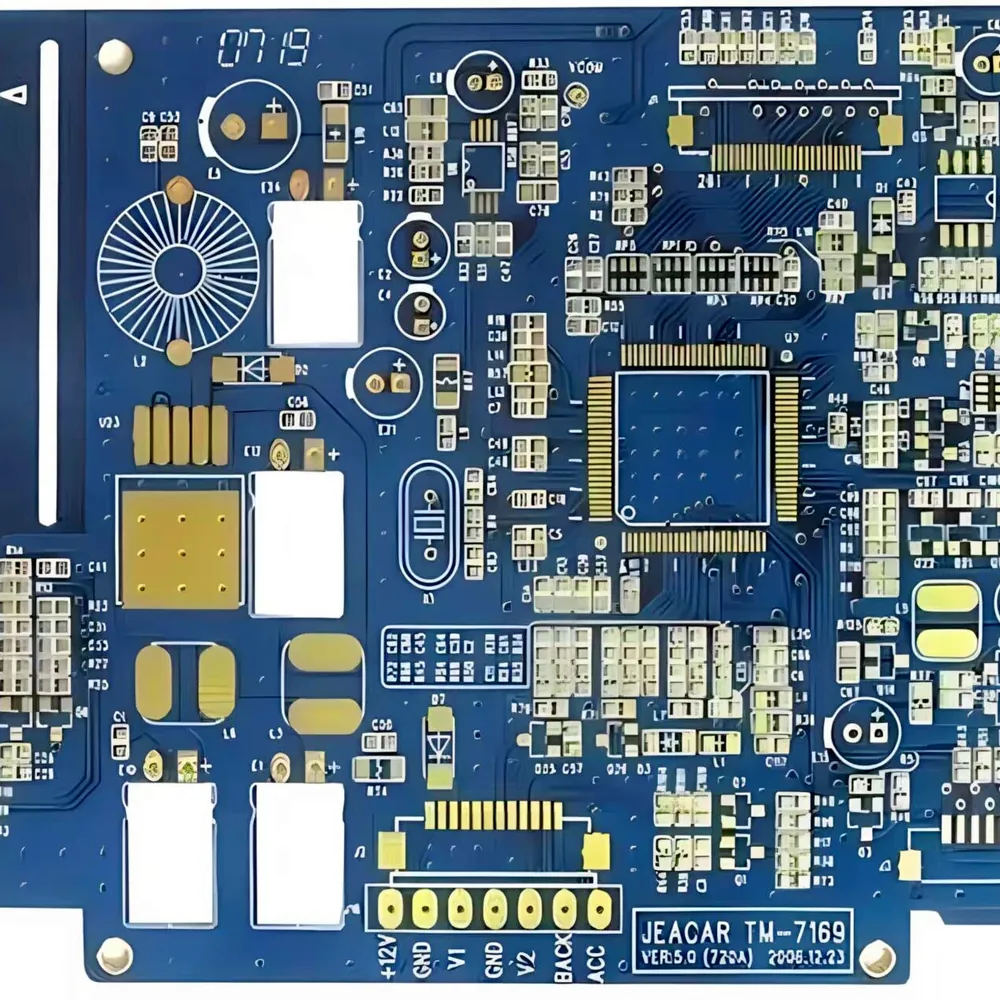
Service overview
Controlled impedance PCBs require agreement on dielectric thickness, copper weight, reference planes, trace geometry, and acceptable tolerance before CAM—not after first article. A layout with correct-looking widths but wrong dielectric assumptions will fail tuning even when the board matches the Gerber.
MOZPCB reviews impedance tables alongside fabrication data: which layers reference which planes, whether coplanar or microstrip structures apply, and whether differential pairs need gap control as well as width. We panelize test coupons when the RFQ requires evidence, and we document the stackup the quote assumes.
Programs range from single 50 Ω lines on a 4-layer board through multi-gigabit differential pairs on 10+ layer stackups and RF-adjacent digital sections on hybrid laminates. Tighter tolerances are available when the geometry and material set support them—stated explicitly in the quote rather than implied.
What we offer
- Stackup design assistance aligned to your impedance targets
- Single-ended and differential pair control with documented tolerances
- Microstrip, stripline, and coplanar waveguide geometries
- Test coupon design and panelization for measurement
- TDR reports on agreed builds when required
- Hybrid stackups combining FR-4 and controlled-Dk laminates
- DFM feedback on reference plane continuity and return-path breaks
- Coordination with assembly finish and reflow plans that affect impedance
Technical capabilities
- Typical tolerance ±10% standard; ±7% and ±5% reviewed per construction
- Dielectric thickness control through agreed laminate sets
- Line width and space limits tied to copper weight and imaging capability
- Coupons on production panels or dedicated test panels per agreement
- Back-drilling for stub reduction on thick high-speed builds
Common applications
- High-speed digital backplanes and switch fabrics
- DDR and SerDes channels on dense mainboards
- Ethernet, USB 3.x, and PCIe routing
- RF-adjacent digital sections requiring stable Dk
- Industrial vision and acquisition with long matched pairs
How the process works
- 01
Requirements intake
Share Gerber, BOM, drawings, quantities, and any reliability or compliance notes.
- 02
Technical alignment
We confirm materials, finishes, assembly flow, and test expectations with you.
- 03
Production & inspection
Manufacturing and assembly follow the agreed traveler with documented checks.
- 04
Delivery
Packing, labeling, and shipment according to your logistics instructions.
Fabrication & impedance coupons
-
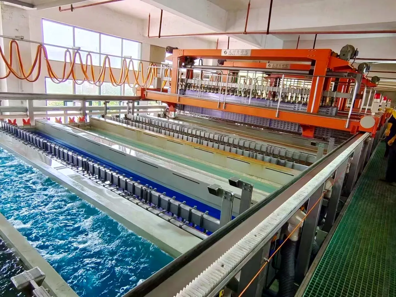
Plating line -
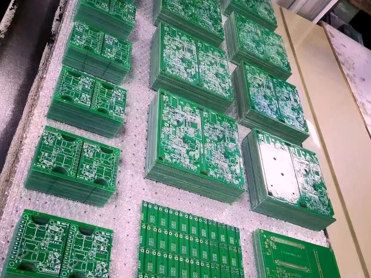
Panelized boards -
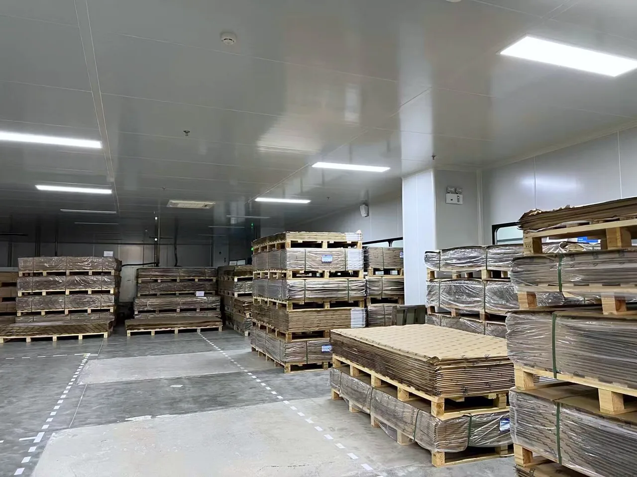
Laminate store
Related services
FAQ
What should an impedance table include?
How tight can impedance tolerance be?
Do you provide TDR reports?
Does surface finish affect impedance?
Get started
Ready for the next step?
Send your project files and requirements. We will review stackup, assembly, and test needs, then respond with a clear quotation path.